方言を話すおしゃべり猫型ロボット『ミーア』をリリースしました(こちらをクリック)

PCB

Development/Design

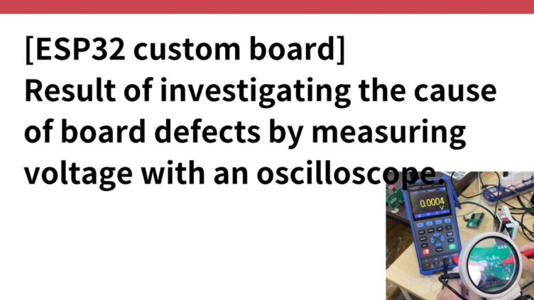
[ESP32 custom board] Result of investigating the cause of board defects by measuring voltage with an oscilloscope.

When wiring voltage is to be measured, the wiring on the board is often covered with resist (insulation layer), so voltage cannot be measured by applying a probe over the wiring as it is, so lightly scratch the area to be measured with a cutter to expose the copper foil part before measuring the voltage.
built-in(C++)

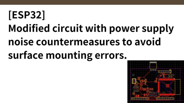
[ESP32] Modified circuit with power supply noise countermeasures to avoid surface mounting errors.

The MAX98357 itself needs to be connected to pins 25, 26 and 22 of the ESP32 WROOM 32E. keep the I2S signals (BCLK, LRCLK and DIN) as close as possible to pins 25 and 26 of the ESP32, as keeping the wires short reduces the risk of signal degradation and cross-talk. Attempt to optimise decoupling capacitors in the circuitry around the power supply to reduce power supply noise.
built-in(C++)

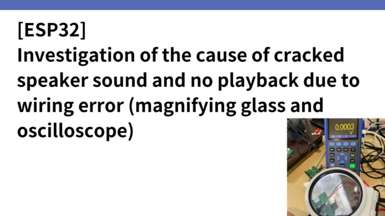
[ESP32] Investigation of the cause of cracked speaker sound and no playback due to wiring error (magnifying glass and oscilloscope)

When the IC package of the Class D amplifier was changed from TQFN to WLP, 4 out of 25 were defective in the speaker area as follows. Investigate the cause of sound crackling and audio not being played back. Verify if the sound crackling is resolved by first lowering the volume in the application. Next, using a magnifying glass, visually check for wiring defects.
Development/Design

Create PCB by EasyEDA and order PCB by JLCPCB. If you want to keep costs down, request 2 boards to be mounted.

Create schematics in EasyEDA and convert the schematics to PCBs Work on the PCBs includes component placement, number printing, board outline drawing, wiring with auto routing, creating mounting holes and creating solid copper foil After completing the work on the PCBs, order the boards from JLCPCB.
Development/Design

[JLCPCB] I received a confirmation email after ordering 100 boards. PCB operation is not checked

If there is no problem with the PCB layout, you will not receive an email from JLCPCB, so if you receive an email, it is when there is a problem, such as an incomplete circuit. Also, JLCPCB does not check the functionality of your own PCB, so you need to look at the schematic and PCB yourself to determine if the order is correct.