Introduction.
Developing “Mia,” a talking cat-shaped robot that speaks various dialects.

In a previous article here, we described an investigation into the cause of surface mount errors by JLCPCB.
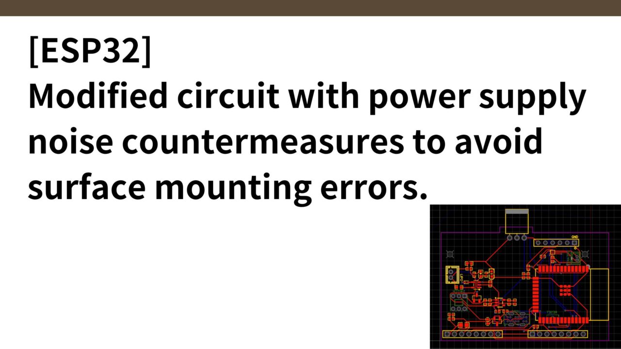
In this article, I would like to describe how to modify the circuit to cause as few surface mounting errors as possible.
By the way, here is the current circuit
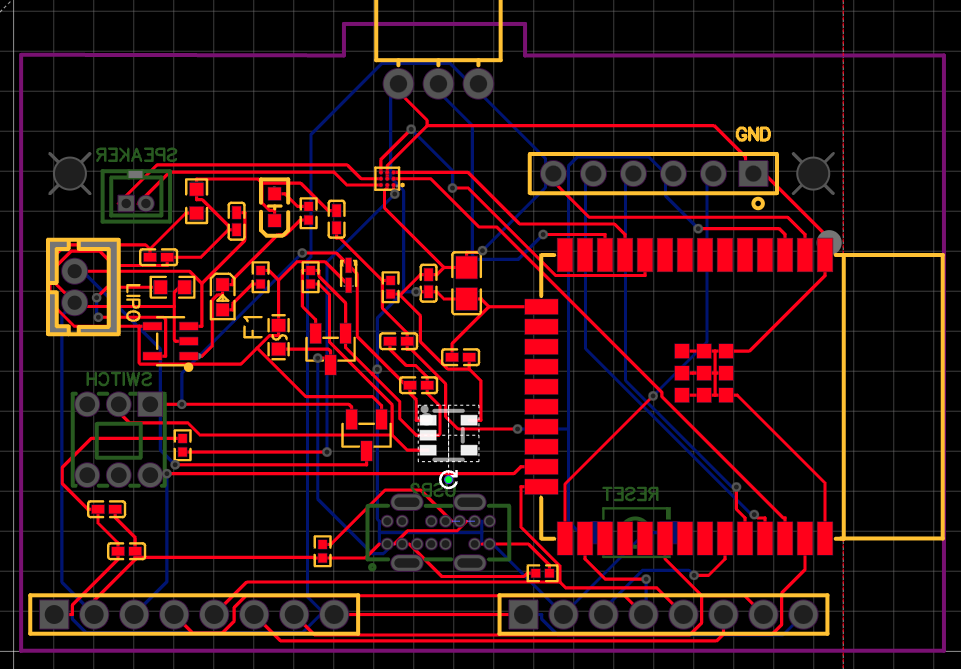
The JLCPCB article describes PCB wiring mistakes that beginners can easily make.

MAX98357 Shorten signal lines around
Change the position of MAX98357 so that the I2S signal wiring is shortened.
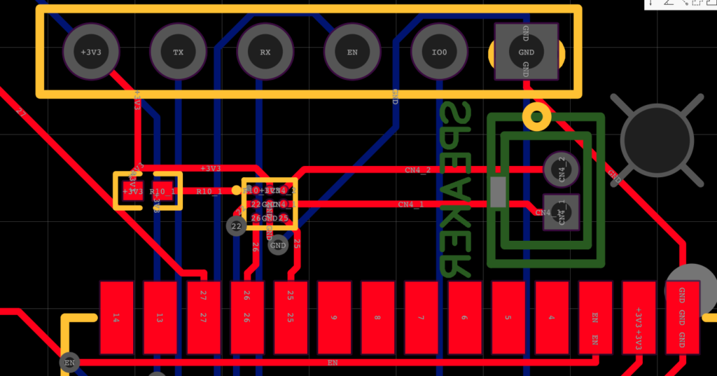
The MAX98357 itself needs to be connected to pins 25, 26, and 22 of the ESP32 WROOM 32E. The I2S signals (BCLK, LRCLK, DIN) should be wired as close as possible to pins 25 and 26 of the ESP32, as keeping them short will reduce the risk of signal degradation and crosstalk.
I put it here to try it out.
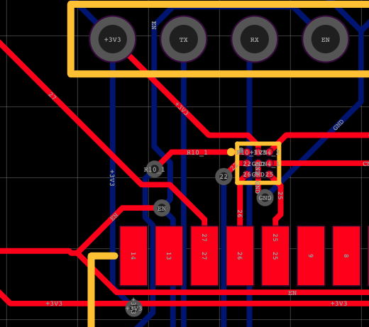
Bring speakers into close proximity
Speaker does not have to be in this location, try to get closer to MAX98357
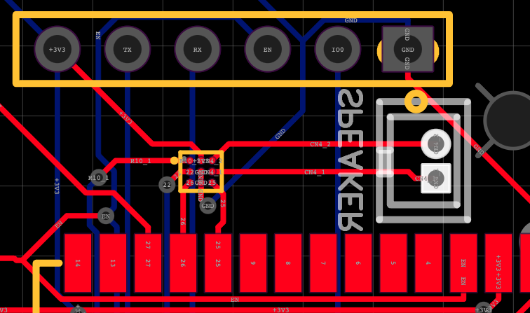
Resistors and capacitors are also placed in close proximity.
R10 resistor is also brought into close proximity.
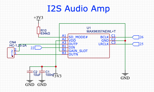
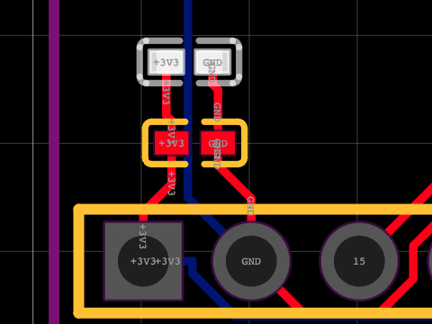
Since the capacitors C1 and C2 connect GND and 3.3V, it was determined that the LCD display pin header on the bottom left of the original board is fine.
Finally, the speaker-related wiring ended up looking like this. I think it was pretty clear.
Optimization of decoupling capacitors
Attempt to optimize decoupling capacitors in circuits around the power supply to reduce power supply noise.
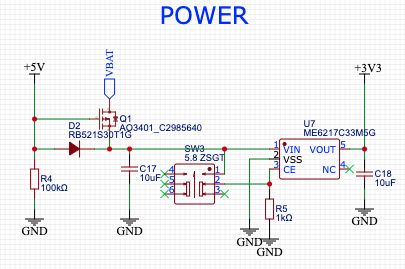
Decoupling capacitors of C17 (10uF) and C18 (10uF) are placed, and an additional 0.1uF ceramic capacitor is added directly to the power pins of each IC. A combination of 10uF and 0.1uF is recommended to effectively eliminate high-frequency noise in particular.
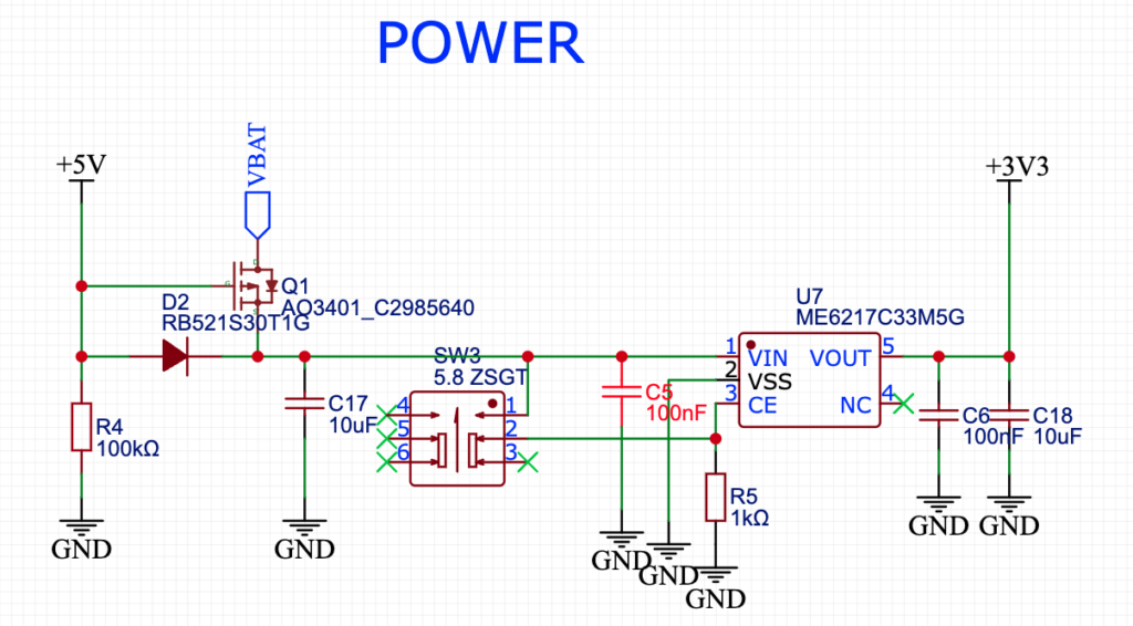
Place the decoupling capacitors, including the newly added 0.1 μF capacitor, as close as possible to the power supply pins of the IC (in this case, U7 (regulator) and Q1 (MOSFET)). If they are placed far away from the power supply pins, the noise rejection effect may be reduced.
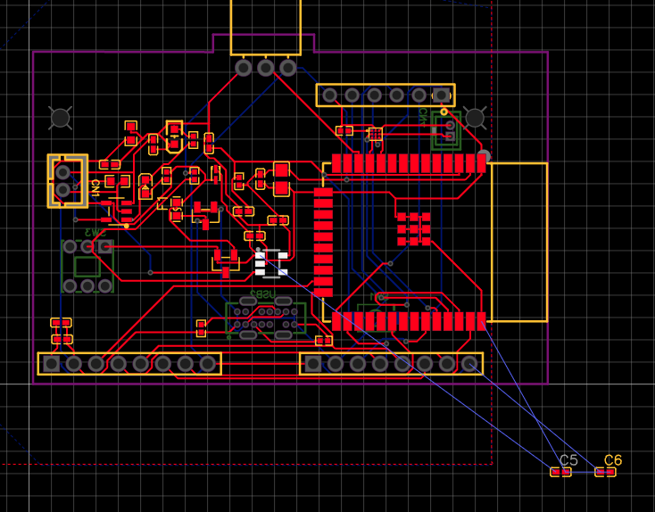
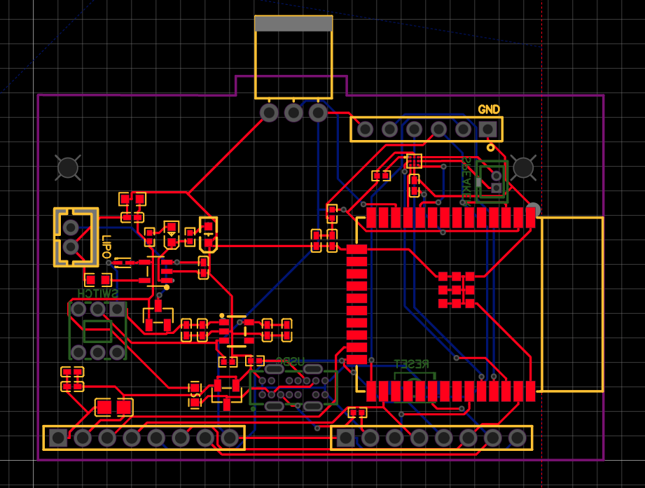
Here is the result of the whole thing, with all the modifications.

It looks much cleaner than the first wiring.

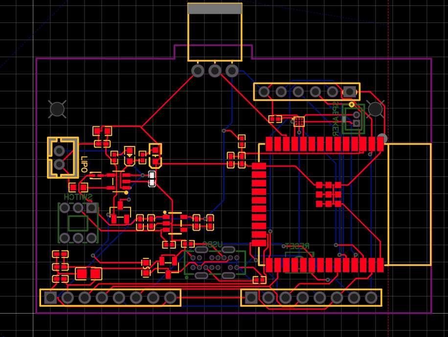
GND line
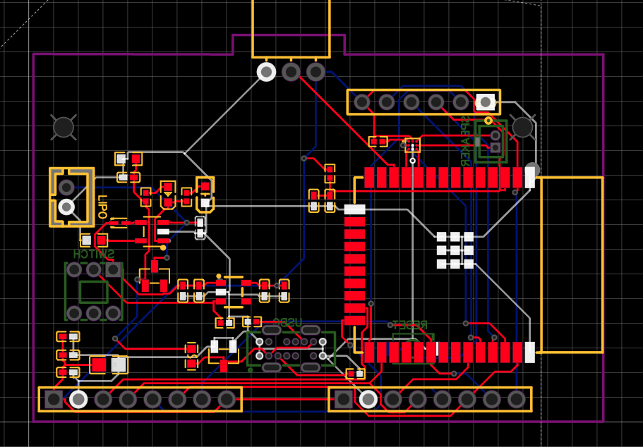
3.3V (after LDO from 5V. ESP32 and LCD display supply power)
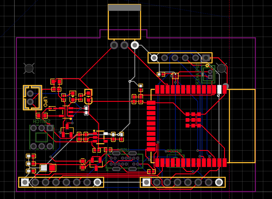
5V line (before USB power supply LDO)
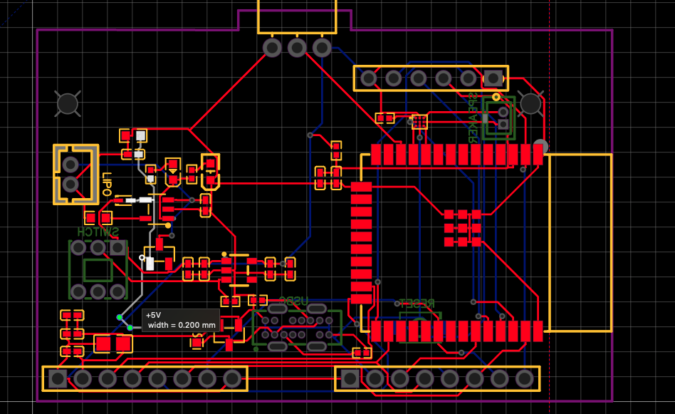
VBAT line (when powered by LiPo)
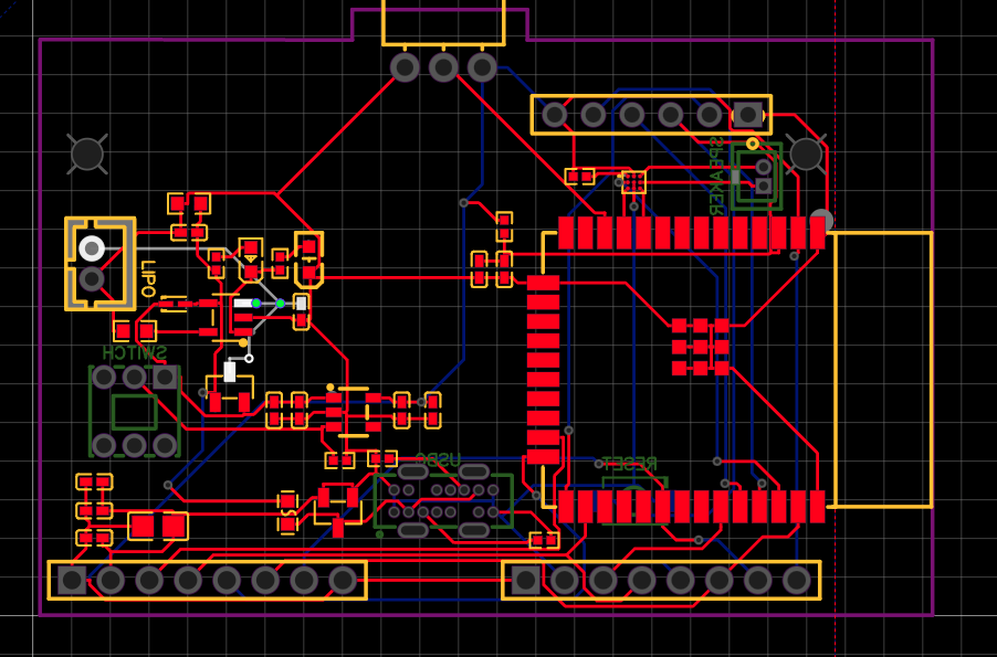
I threw it to ChatGPT and got the following reply
I checked the new wiring layout. Overall, it is tidy and appears to be well secured with power and ground lines. Each layer of power lines is separated by layer and appears to be carefully designed for noise suppression, but a few points could be further optimized. We comment on each point below.
It is better to put the decoupling capacitor as close as possible to the I2S amplifier, so we moved the capacitor with the previous statement
When I moved only the 0.1μF capacitor closer to MAX98357A and increased the Track width from 0.2mm to 0.25mm, only one wire failure occurred between MAX98357A and the capacitor.
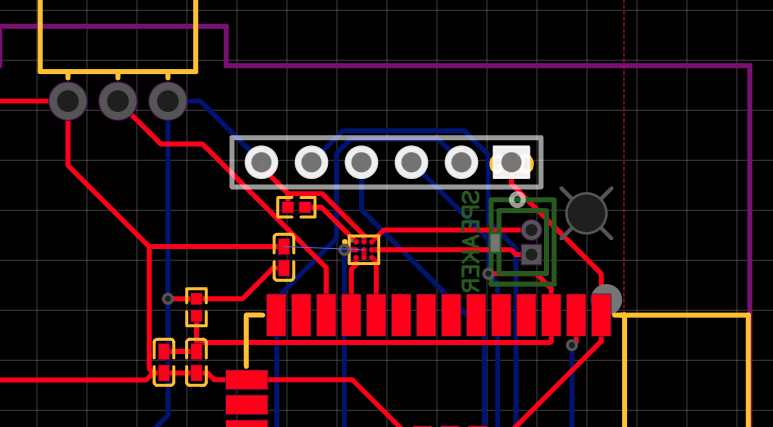
Track width was set to 0.23mm, success. track clearance is 0.16mm
The wiring distance between the MAX98357A power supply pin (VDD pin) and the 0.1μF decoupling capacitor was placed as shown below to minimize the distance. The decoupling capacitor was able to be placed close, but on the other hand, the signal line No. 25 became a little longer than the shortest distance.
The question arises as to which should be prioritized, but since it is better to prioritize the noise immunity of the entire circuit and the stability of the power supply, we decided to use the modified arrangement.
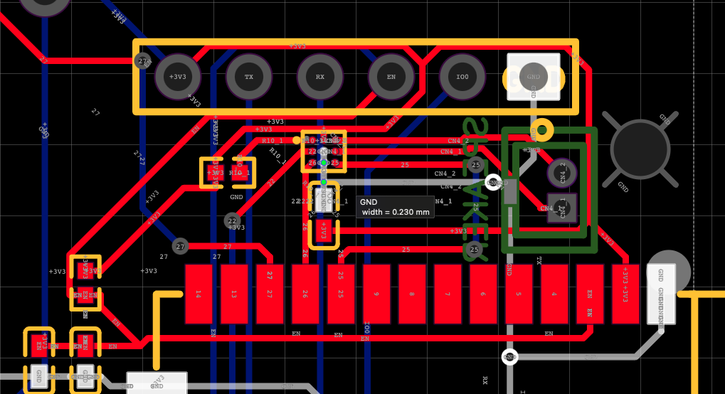
The final circuit is here.
The wiring around the MAX98357A IC is a bit complicated, and I am concerned about another surface mounting defect, so I will add a comment when I place the order, “Since the MAX98357A IC package is small and the wiring is dense, please pay special attention to the wiring around the IC.
