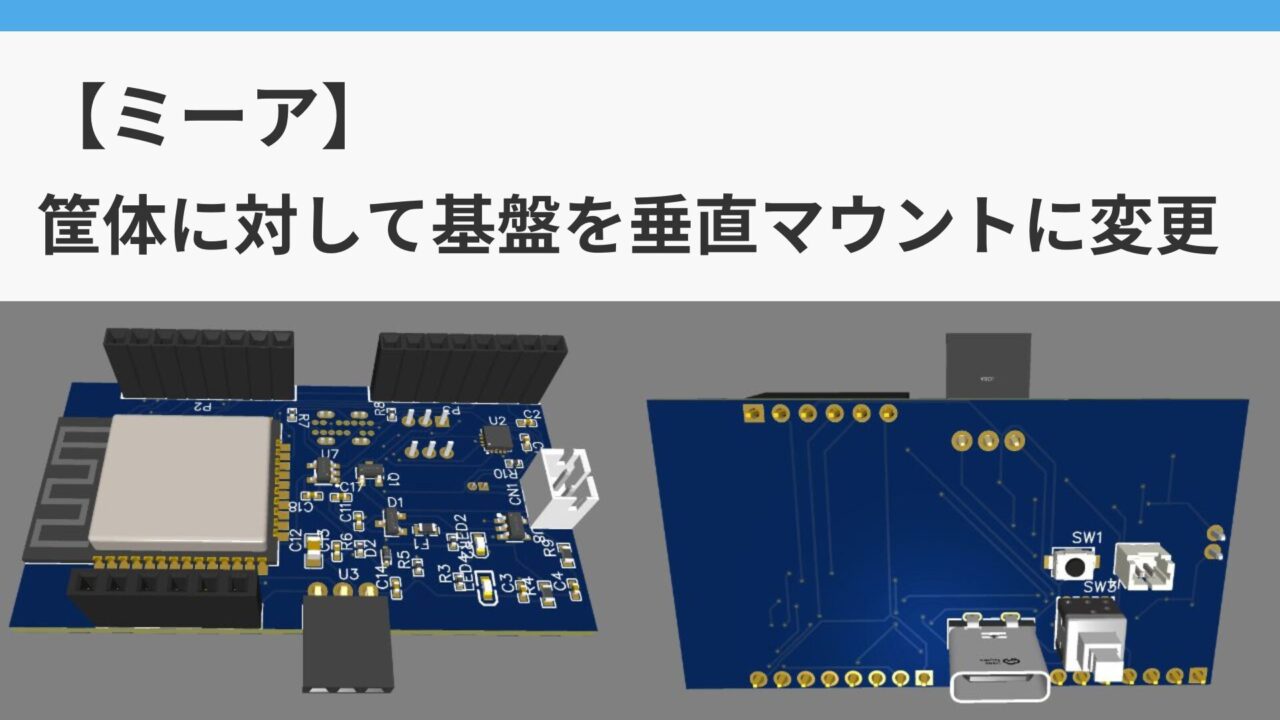
Both the hardware and software of the chatty dialect-speaking cat robot “Mia” under development will be released on June 1st. Even during Golden Week, I was absorbed in development.
I also ordered 105 self-made boards from JLCPCB, but I received an email confirming the installation, so I will write about the exchange this time.
Contents of confirmation email from JLCPCB
Currently, the circuit diagram for the board is created using EasyEDA, and the PCB is ordered from JLCPCB. This combination is probably the easiest and relatively cheap at present.
Previously, I used KiCad for board design CAD, but now I use EasyEDA exclusively.
This is the first time that we have ordered as many as 100 self-made boards. Until now, it was just for testing and verification, so I had repeatedly ordered only two units for testing.
If the board that arrived didn’t work after we ordered it, the cost would have been too high, so we ordered 100 units using the circuit diagram that we had confirmed worked properly in advance.
So I thought there would be no particular problem, but then I received the following email.
Dear customer,
Well got your order with many thanks.
Sorry to bother you, but there is one thing that we want to confirm with you about your SMT order before proceeding.
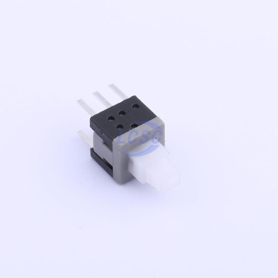
For part C2681587, see Figure 1 and Figure 2 which is correct.
Your early reply will be highly appreciated, thank you so much!
Figure 1 Figure 2
JLCPCB does not verify circuit diagrams.
If there is no problem, you will not receive an email from JLCPCB, so if you receive an email, it means there is a problem such as a defective circuit. When I receive an email, I get nervous.
Regarding latching switches, I once received the following message when I placed an order, and as a result, due to my mistake, I received a board with a power supply that did not work.
Regarding this time, I was asked to tell me which direction is correct for the latching switch, up or down.
I thought maybe I made a mistake in the circuit diagram, so I replied below.
Dear Customer,
Thanks for your message
Does this mean that the power supply does not work properly with my current latching switch?
Here is the circuit diagram I created, which specifies that no current flows to the LDO when the switch is switched off, and that current flows to the LDO when the switch is switched on and the power supply is switched on
Best Regards,Kazutaka
I received the following reply.
Dear Kazutaka,
Unfortunately, we do not perform functional testing on customer boards. Could you please advise us on how to solder part C2681587 according to your design?
We look forward to hearing from you. Best regards,
JLCPCB does not check the functionality of self-made boards. So, please look at the circuit diagram and PCB and make your own decision.
There seems to be no problem even if the latching switch is upside down.
So, check the circuit diagram and C2681587 parts
The latching switch is the part labeled “SW3” in the circuit below, but is it correct if pins 1, 2, 3 and 4, 5, 6 are reversed or in the order shown in the circuit diagram? I guess you want to make sure.
In this case, only one side of the latching switch is used, and the left and right sides are symmetrical, so it seems that either Figure 1 or Figure 2, as pointed out by the JLCPCB, will work normally.
Just to be sure, check the C2681587 part at LCSC. Functionally, it’s symmetrical, so it seems like there’s no need to make a recess on one side, but why?
Just to be sure, I ordered two homemade boards with the same circuit diagram and checked the latching switch on the one I had on hand. There is a recess toward the outside of the board, so it seems to correspond to Figure 1.
So, I sent the following reply.
Dear Customer Support,
Thank you very much for your reply.Regarding the weld orientation on part C2681587, please proceed with the direction shown in Picture 1.
Thank you for confirming this detail for us.
Best regards,Kazutaka
Why did I receive a confirmation request only this time?
In the first place, the last time I placed a test order for just two units with the same PCB layout, I didn’t receive a confirmation request, so why did I receive a request this time?
Refer to the 2D drawing of the component placement of the PCB layout ordered from JLCPCB. I won’t know for sure until I see it in 3D, but there was probably no information about the dent in the latching switch in the component layout, but when I tried to actually surface mount it, the C2681587 part had a dent on one side, so I requested confirmation. It must have come.
In theory, it should work properly with the boards that will arrive, but since I received this confirmation request, what should I do if all 100 units don’t work? I’m a little anxious as I wait for it to arrive.


コメント