Talking cat-shaped robot “Mia” that speaks various dialects is under development.

I have programmed it to talk when you pat it on the head, but since I am using a MAX98357 in the speaker’s amplifier, I will describe the two MAX98357A packages and their wiring.
Enable speaker drive even with Lipo power supply
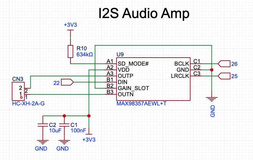
Here is the circuit of my current Audio amp. The input power supply is still 5V, so USB power supply will drive the speaker, but if I change to lithium battery, it will not drive the speaker because the input voltage is 4.2V at maximum.
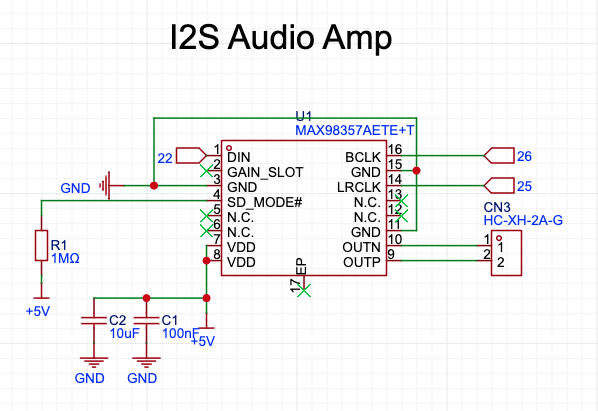
The MAX98357A datasheet allows an input voltage of 2.5-5.5V, so we will change the input voltage to 3.3V.
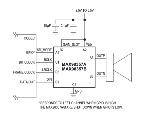
MAX98357A WLP package compared to TQFN
The MAX98357A series of ClassD audio amplifiers includes the following two
- WLP Package ( Wafer Level Package: MAX98357AEWL+T): 9-pin
- TQFN package (MAX98357AETE+T): 16-pin
The WLP package is smaller and more cost effective than the conventional TQFN package, as it does not require expensive through-hole vias (connection pins that pass through the PCB). This reduces the size and pin count of the IC, enabling miniaturization while lowering manufacturing costs.
Incidentally, we have been using a 16-pin TQFN package.
In fact, the WLP package is slightly cheaper than the IC alone.
MAX98357A WLP GAIN pin handling
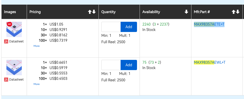
The following is a detailed explanation of the WLP package’s handling of GAIN.
The WLP package has the following 9-pin structure, and the GAIN pin that controls the volume is located in the middle of the 9 pins, which raises the question of how to wire this if it is used.
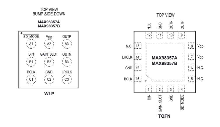
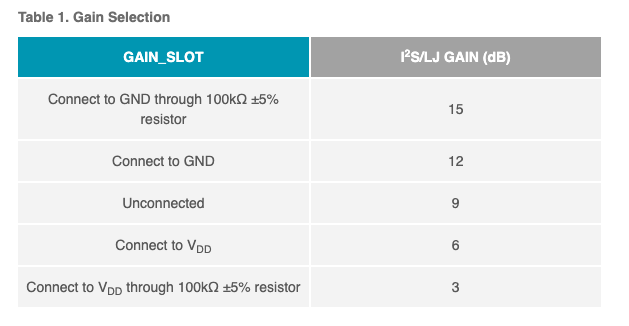
It is recommended that the GAIN_SLOT pin be digitally controlled to adjust volume instead of analog control, which would eliminate the need for a new route for the GAIN_SLOT pin and allow for more precise volume control.
Time-Division Multiplexing (TDM) mode is used when multiple audio channels need to be transmitted and processed simultaneously. When processing a single audio stream from a single input audio file, TDM mode is usually not needed. Note that in TDM mode, Gain is fixed at 12 dB.
In the I2S mode (Inter-IC Sound) used in this case , the GAIN_SLOT pin can be used to set the output speaker volume. In this case, we will connect the GAIN_SLOT pin internally to GND and set the output to 12 dB.

SD_MODE: How do I output both channels on one speaker?
Used to turn on/off the IC and for channel selection.
When the SD_MODE pin is connected to a low voltage (e.g., GND), the IC is in shutdown mode (off state), and when connected to a high voltage (e.g., VDD), the IC is in normal operating mode (on state).
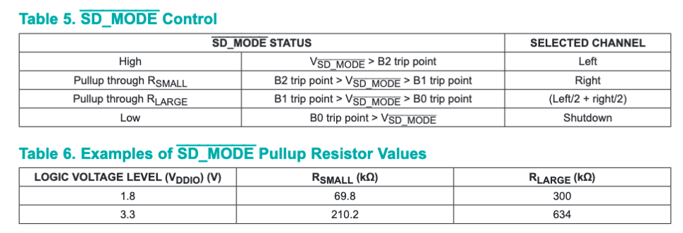
Channel selection can also be made using a pull-up resistor on the SD_MODE pin, which controls the voltage level on the SD_MODE pin and tells the IC which stereo channel to process; a high voltage on SD_MODE selects the left channel, a high voltage through a small resistor selects the When SD_MODE is set to a high voltage through a small resistor, the right channel is selected, and when set to a high voltage through a large resistor, both channels are selected. In this way, the operating mode of the IC is determined based on the voltage level.
In this case, we want to use one speaker and mix both channels (left + right). This will allow us to combine the sound information from both left and right stereo sources and maintain some depth and spatial extension of the music or voice.
According to the table, the channels should be Left/2+Right/2, so the SD_MODE pin should be supplied with a high voltage through a large resistor value.
The formula is RLARGE (kΩ) = 222.2 x VDDIO – 100, where VDDIO is the logic voltage supplied through the digital interface to the chip or IC. This time, the input voltage is 3.3V, changing from 5V, so VDDIO is 3.3V as well.
RLARGE (kΩ) = 222.2 x 3.3 – 100 ≈ 634 kΩ (already listed in the table as an example) must be connected as a pull-up resistor.
Speaker requirements to be connected
Recommended speakers have a series inductance of 10 μH or greater (a characteristic that slows the flow of current and affects the processing of audio signals).
Higher inductance allows the voice coil to respond better to changes in current and reproduce sound more accurately; values above 10 μH help improve the quality of the speech signal.
A typical 8 Ω speaker exhibits series inductance in the range of 20 µH to 100 µH, so it meets this requirement.
By the way,
The ohms (Ω) listed on the speaker represents the resistance of the speaker; lower values require more current but can provide higher sound volume. Higher impedance makes the sound quieter but cleaner with less noise.
W (watt) indicates the maximum power a speaker can handle, with higher wattage meaning louder volume.
So I changed to MAX98357A WLP package like this.
Routing is very difficult.
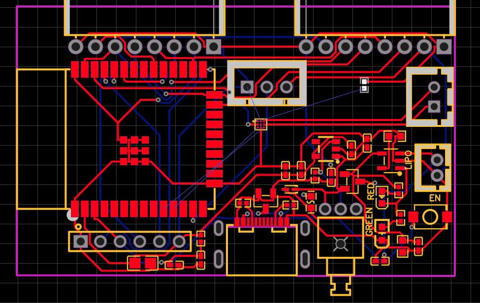
After changing to the WLP package, routing errors occurred in the wiring around the WLP package even with auto routing, making it difficult.
I tried several times, but I had to connect the GPIO 25 and 26 pins of the esp32 wroom 32E module and the GPIO 22 pin on the opposite side, and the size of the board is getting smaller, so it is difficult to solve the routing error.
As a future issue, PCBs are made and ordered with the conventional TQFN package.
After deauto routing the TQFN package, I was able to create it in one shot with failure 0.
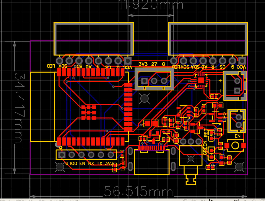
P.S. After that, we ran into a TQFN package out-of-stock problem, and here is an article on how to change the Track Width and Clearance settings to enable wiring in the WLP package.


コメント