Currently developing “Mia,” a talking cat-shaped robot that speaks dialect.

In order to create Mia’s custom board (ESP32-based), I thought I had to first understand the schematic of the ESP32 development board, and when I started looking at it, I came across the following schematic and truth table and thought, “What the heck.
I started to investigate the following circuit as it corresponds to the automatic bootloader function of ESP32, but it took me 6 or 7 hours to understand it because I had to go back to the basics such as transistors and pull-up resistors after studying schematics for the first time in a long time.

In this issue, I would like to describe my understanding of how the ESP32 automatic upload function works. If you find any mistakes, we would appreciate it if you could point them out to us in the comments section.
UART flow control
First, UART stands for Universal Asynchronous Receiver/Transmitter.
There are two methods of transmitting digital signals: parallel and serial communication, and within serial communication there are synchronous and asynchronous types. UART falls into the asynchronous type of serial communication.
When exchanging data between two devices via UART, if data is sent from the other device when the device is not ready to receive the data, it will miss receiving the data. To prevent this from happening, the sending device is notified to “wait a moment before sending data,” and the data flow is adjusted by temporarily suspending transmission or slowing down the speed. There are several methods of flow control, but the one that concerns us this time is hardware flow control.
- Sender: When the sending device wants to send data, it sets the RTS line High
- Receiver: When the RTS line goes High, the receiving device checks if it is ready to receive data from the sending device. If ready, the CTS (Clear to Send) line goes High to notify the sender of permission to send.
In this case, we assume that the program is written from the PC (sender side) to the ESP32 (receiver side) via USB.
- The PC (sending side) prepares the program data to be written to the ESP32, and when it is ready for communication, it sets DTR High to notify the ESP32 that “communication is ready”.
- When the ESP32 (receiver) detects the DTR, it knows that the sender is ready to accept communication.
- After communication is established, when the PC wants to send program data, it sets RTS High to signal “ready to send”.
- When ESP32 detects RTS, if the buffer is free, it raises CTS to High and notifies PC of “ready to receive”.
- The PC starts transmitting program data when CTS detects High.
- When the ESP32 buffer is full, CTS is set Low to notify “reception pause”.
- When the PC detects a Low on CTS, it suspends data transmission.
- When the ESP32 buffer is free, CTS is again set High to notify “resumption of reception”.
- The PC resumes data transmission, and when all data has been sent, DTR is set Low to signal “end of communication”.
First, the DTR tells the receiving terminal that communication has been established, and then the RTS asks the receiving terminal if it is OK to send data. Without establishing communication first, data cannot be sent in the first place, and even if communication is established, if the receiving terminal does not have the capacity to accept the data, it will be overflowed, so the two-step process is to ask if it is OK to send the data now.
EN pin and IO0 pin of ESP32
EN pin: Button for restart, abbreviation of Enable
- High: Normal operating mode. When the EN pin goes High, the ESP32 recovers from reset and starts normal operation.
- Low: The ESP32 enters a reset state. When the EN pin goes Low, ESP32 experiences a hard reset and all operations stop.
- Press when the program is re-run or behavior becomes unstable.
- There is no built-in pull-up resistor.
IO0 (Input/Output 0) pin
- High: In normal execution mode, the program stored in flash memory is executed.
- Low: Boot loader mode (also called flash mode), enters a special mode to write a new program to flash memory; ESP32 is ready to accept program writes.
- It has a pull-up resistor built in, so it is normally High.
So, when you want to write a new program to ESP32, you can do so by pressing the switch buttons in the following order.


- ラベルタイトル
- ラベルタイトル
- ラベルタイトル
- ラベルタイトル
The above is just an example. To be precise, if I0O=EN=Low is maintained and only EN switches to High, that moment is detected as the boot loader mode and programming can start. It is fine as long as I0O=EN=Low state is maintained.
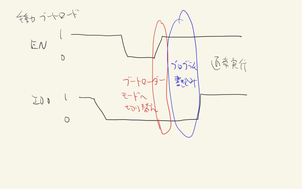
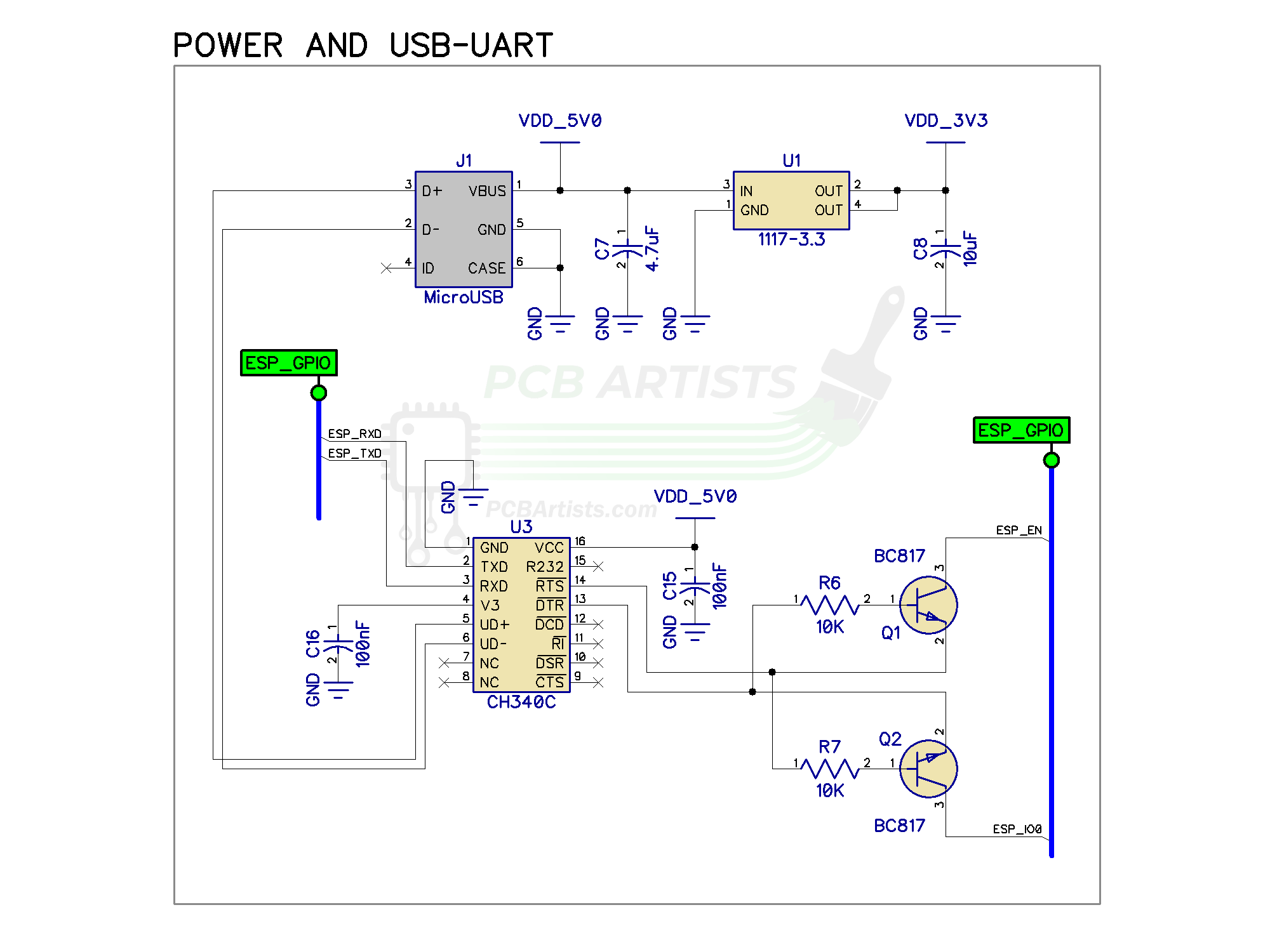
Automatic Boot Loader and Truth Table
Now, finally, we would like to look at the schematic and truth table here.
First, 0 and 1 in this truth table represent the following, respectively.
1=High=Positive voltage (+5V or +3.3V)
0=Low=0V
This figure and the truth table show that by using the host PC program to adjust the voltages on the DTR and RTS pins of the USB-UART conversion chip, respectively, to create the state (DTR, RTS)=(1,1)(0,0)(1,0)(0,1), and also by using the two transistors (Q1, Q2) well, This shows that the EN and IO0 voltages can be well adjusted.
Role of Transistors
The transistor used here is an NPN transistor.
For more information on the role of transistors, please refer to the following article.

When DTR=1, RTS=0
Since it is an NPN transistor, current flows from the base (DTR) to the emitter (RTS) and also from the collector (EN) to the emitter (RTS).
The emitter is RTS and is 0V, so when current flows from the collector to the emitter, the collector is also 0V, so EN = 0V, which is 0 in the truth table.

On the other hand, since the voltage of the IO0 pin is DTR > RTS, no current flows from the base (RTS) to the emitter (RTS) of Q2, so of course no current flows from the collector (IO0) to the emitter (RTS). So, it would be 0V, but since the IO0 pin has a pull-up resistor inside the ESP32 unlike the EN pin, it becomes 3.3V, which is 1 in the truth table.
For more information on pull-up resistors, see the following article
https://voltechno.com/blog/pullup-pulldown/
In the state of DTR=1, RTS=0, the transistor of Q2 does not flow current between the collector-emitter, so the switch can be regarded as open, the IO0 pin is in the following state, and since the internal resistance of ESP32 is very large, it can be pulled up to 3.3V from the voltage divider principle The voltage divider principle is used to pull up to 3.3V.

It was found that by creating the DTR=1, RTS=0 state in the PC program, it is possible to create the EN=0, IO0=1 state (= state to start writing the program).
When DTR=0, RTS=1
Since this is the reverse of the previous state, current flows from the base (RTS) to the emitter (DTR) and also from the collector (I0O) to the emitter (DTR).
The emitter is DTR and is 0V, so when current flows from the collector to the emitter, the collector is also 0V, so IO0 = 0V, which is 0 in the truth table.

On the other hand, EN is supposed to be 0V since there is no current flow to the Q1 transistor = the switch is open, but since a pull-up resistor (10kΩ) is attached to the wiring leading to EN and connected to 3.3V, EN = 3.3V, which is 1 in the truth table.
The IO0 pin has a pull-up resistor inside the ESP32, so there is no need to install an external pull-up resistor, but the EN pin has no pull-up resistor, so a pull-up resistor must be installed outside if the above truth table is to be achieved.
Further capacitors between EN pin and GND?
Now we know that we can achieve the truth table, but what we want to do is to be able to automatically write the program when we instruct the PC to write the program (by pressing the Upload button on PlatformIO) without having to manually press the EN or BOOT pin (IO0 pin).
A necessary and sufficient condition is to create the state (EN, IO0) = (1, 0) from the state (EN, IO0) = (0, 0). Since this moment is recognized as a program write.
Based on this, if we look at the previous truth table, we can see that (EN, IO0) = (1,0) can be achieved by controlling DTR and RTS, but (EN, IO0) = (0,0) cannot.

And how is this solved in the official Espressif documentation?

If this circuitry is implemented (all Espressif boards have it), adding a capacitor between the
EspressifENpin andGND(in the 1uF-10uF range) is necessary for the This is shown in the ESP32 Module section of the schematic.
It is stated as follows. It means that you should put on the capacitor as follows.

I asked Chat-GPT and received the following response
Capacitor: A 100 nF capacitor is responsible for controlling the timing of the reset. This capacitor temporarily extends the time that the EN pin goes Low to ensure that the ESP32 is reset.
Below are the details of this operation.
- At reset: When DTR=1, RTS=0, the transistor is turned on and the EN pin is pulled low. At this time, the capacitor is discharged.
- After reset: Switching DTR=0, RTS=1 turns off the transistor and the EN pin is pulled High by the pull-up resistor. However, there is a slight delay before the EN pin goes High because the capacitor is temporarily discharged.
- Programming Mode: This delay ensures that the ESP32 enters programming mode in synchronization with when IO0 goes Low.
This design is used to adjust the timing of reset and switching to programming mode to make the programming process reliable and trustworthy. The capacitor value is chosen to regulate the timing of the reset. If this value is too large, the reset may be too late. If it is too small, the reset may not be performed fully.
I think the illustration would be something like this.

When switching between DTR and RTS with no capacitor, the IO0 pin cannot enter programming mode because the EN pin goes from 0 to 1 at the same time the IO0 pin goes from 1 to 0.
So, even if the voltage on the EN pin rises from 0V to 3.3V by connecting a capacitor between the EN pin and GND
- Transistor turns OFF: When DTR goes Low and RTS goes High, the transistor turns OFF. At this time, current from the collector to the emitter stops flowing.
- Rising voltage on the EN pin: When the transistor is turned off, the EN pin is pulled high by the pull-up resistor. However, the rise of the voltage is slow because the capacitor is in a state of charge.
- Capacitor charging: Since the capacitor is connected in parallel with the EN pin, there will be a time when the voltage on the EN pin is held at 0. This time depends on the capacitance of the capacitor and the value of the pull-up resistor.
This behavior creates a slight delay in the time it takes for the voltage on the EN pin to go High, creating a state where IO0 = EN = 0, and then only EN goes to 1, allowing programming writes. I understood that.
What is the recommended capacitor capacity?
If the capacitor’s capacitance is too small, the time that EN = 0 is held down will be too short, and it may not be possible to create the EN = IO0 = 0 state, which is why the capacitor should be 1 μF or larger. On the other hand, if the capacitor capacitance is too large, the state of IO0=EN=0 will be too long, and the program writing will not be able to start no matter how long it takes (I did not go any deeper here, but will the timeout message appear as if the program writing cannot start? (I didn’t go any deeper than this, but I’m getting a Timeout message like I can’t start writing the program?) I’m not sure if this is the case or not.
The same Espressif formula has
Some third party ESP32 development boards use an automatic reset circuit for
EspressifEN&GPIO0pins, but don’t add a capacitor on theENpin. Adding a 1uF (or higher) value capacitor betweenENpin andGNDmay make automatic reset more reliable.
and when creating a home-made custom board, etc., it was stated that a Capacitor of 1μF or more should be included, and there was no mention of an upper limit. However, in the ESP32_DevKitC_V4 schematic, the Capacitor connected to GND is 0.1μF, which is 1/10 of the lower limit stated in the official description, which is a mystery.
Also in the following article
EN pin needs capacitor of at least 100nF and a pull-up of at least 10K for auto-program circuit to work!
ESP32 CH340 PROGRAMMER SCHEMATIC
It is stated that 0.1 μF may possibly be sufficient.
So, since it had been a while since I had done a schematic, I had to start over from the basics, such as the transistor and pull-up resistor mechanisms, and it took me quite a while. But now that I finally understand how the ESP32 automatic bootloader works, I hope to be able to proceed with the schematic of my own board.


コメント