
We are currently developing a talking cat robot called “Mia”.

In this post, I will describe the steps to place an order with JLCPCB after completing the schematic drawing from EasyEDA.
Schematic creation with EasyEDA
This is how the schematic creation was completed!
(In another article, I would like to describe the procedure for creating schematics in EasyEDA)

Convert schematics to PCB
Click “Convert Schematic to PCB” on the Design tab to convert the schematic to PCB.

The “Do you want to check for net errors?” Select “Yes” when you get a warning message.

When executed, one error was displayed in the left sidebar.
I have selected the number 0 as the pin header to connect to the IO0 pin of the ESP32-WROOM-32E, but I am getting angry that there is no number 0 on the pin header side. This time, IO0 is not used as a pin header, but is internally coupled as a Boot switch, so I renamed it to IO0 which is connected as a Boot switch to match.


The internet error was resolved without incident.

Execute “Create PCB from Schematic” again.
This time, it ran without displaying any errors and automatically opened the PCB tab and placed the components! Next, we move on to work on the PCB.

Working with PCBs
Component Placement
First, the components are placed manually.
Place the ESP32 module on the left, pin headers above and below it, and the USB Type C connector on the far right.
Two switch buttons (Reset pin and Boot pin) are placed on both sides of the USB Type C connector.
Place the remaining components (buck regulator, USB-UART conversion driver, resistors, capacitors, etc.) between the USB Type C connector and the ESP32 module.
Below is a development board that supports the ESP32-WROOM-32E, CH340C, and USB-TypeC already on the market. Wiring efficiency should be good, so we will arrange them similarly to this.

The figure below shows the stage where the main components other than resistors and capacitors are placed. Now, capacitors and resistors are placed with the assumption that they will not get entangled when wired.
If the wiring spacing is too narrow and an error occurs when wiring with auto layout later, it is OK to make the resistors and capacitors a little longer horizontally to give them more space.

Resistors and capacitors are also placed

number printing
The ESP32 pin numbers will be printed on the pin headers.
In the PCB Tools panel, select the text mark and drag and drop it onto the board. The text will appear in red text.

In Text Properties, change the text size to the following
Layer: TopLayer→TopSilkLayer (text on the board changes from red to yellow)
Line Width:6mil
Height: 45mil
Good text size.
- Top Layer: The main conductive layer of the substrate. Traces, pads, and other conductive elements are placed
- TopSilkLayer: Non-conductive printed layer on a substrate. Component identification, placement information, text, logos, etc.

Draw a board outline
Select “BoardOutLine” from the All tab in the Layers and Objects panel.

In the PCB Tools panel, select Track and make a stroke to cover the component.

wiring
Click on “Auto Route” on the Route tab to execute automatic routing.

If Auto Route fails, export the Auto Route file (DSN: stands for Design Specifications Network), use a third-party auto routing tool such as FreeRouting to correct the routing, and if possible, import the Session file ( SES) and import the exported completed version to the PCB.
Click Execute.

This time, Auto route succeeded by chance once!

Creation of mounting holes
Create 4 mounting holes on the edge of the substrate.

Copper foil solid preparation
Coat the top layer and bottom layer with solid copper.
First, confirm that the focus is on the Top Layer in Layers and Objects, then select “Copper Area” from PCB Tools, which is marked with a dotted rectangular frame, and create a solid-faced frame that covers the entire substrate.

When clicked, the Properties item pops up. Leave the default GND and click OK.

Click on the Escape button when the entire base is covered, and the entire base will be painted solid red.

Next, select “BottomLayer” in Layers and Objects, and again select the Copper area mark in the same way, and apply a solid coat of paint on the bottom surface as if covering the entire base.


This completes the work at the PCB. Next, we will proceed to the JLCPCB site to order the foundation.
Incidentally, pressing the 3D button gives a 3D view of the substrate.

Ordering substrates at JLCPCB
PCB/SMT orders from EasyEDA
Click on “One-click Order PCB/SMT” in the Fabrication tab

You will get an alert that says, “Do you want to check design rules before creating a Gerber file?” Click “Yes” when you get an alert.

If there are no errors, proceed to the order screen. Select quantity and board color, then click “One-click Order PCB/SMT.

Check PCB Assembly
Then, you are automatically taken to the JLCPCB order screen, which is basically left as it is, since the detailed items for PCB orders are automatically filled in for you.
In this case, we would like you to do PCB Assembly as well, so please check the box. If you only need the PCB and want to do the surface mounting of the components yourself (e.g., to keep costs down), you can skip this step.
The PCBA Qty (number of pieces to be mounted) is set to 5 by default, but you can enter a number between 2 and 5 in the adjacent numeric entry field. If you want to reduce the cost by mounting only 2 pieces for prototyping, enter 2.

Scroll down and click the Confirm button to go to the preview screen, then click Next.

Switch to the “Bill of Materials” tab.
Upload BOM and CPL files
Since we are also requesting PCB Assembly this time, BOM (Bill Of Materials) and CPL (Component Placement List) are also necessary.
Return to the EasyEDA site and output BOM and CPL files.
For BOM files, click “Export BOM” on the File tab, a list of parts will pop up, and then click the Export Bom button.


For CPL files, click on “Export Pick and Place” in the File tab. A check will appear regarding placement mirrors, but this time it is JLCPCB, and in that case, it is stated that the check is unnecessary, so Export is performed as is.


Return to the Bill of Materials tab of the JLCPCB, upload the BOM and CPL files, and click “Process BOM & CPL”.
Then, a message will appear asking if the parts can be procured from the BOM data by JLCPCB. If not, you will get an alert as shown below (e.g., 2 shortfalls), so you need to change the component.

Click on the search icon for the appropriate part. The one they say they don’t have in stock at this time is the female pin header 1 x 6 hole.

Click on the Search Part tab and try entering another LCSC part. Then, this time, there seems to be no alert, so I press the Select button and rewrite.

The changes are reflected and the alert disappears without incident.
Note that the pitch spacing and component sizes must match perfectly or the wiring will be misaligned.

After successfully resolving the error, click Next.

You will be automatically taken to the “Component Placements” tab. After a short wait, the final form with the component on the board will be displayed, and if you are sure, click Next.

Order PCB
You will be taken to the Order screen, select Product Description (required), and click “Save to Cart”.

The final order of 5 boards and 2 pre-mounted components will be displayed, and if there is no mistake, proceed to the payment.

On the last screen of the payment process, you can select a coupon, which you should select.
Basically, every time you place a PCB order, a new coupon is issued, and the system allows you to apply some kind of coupon.

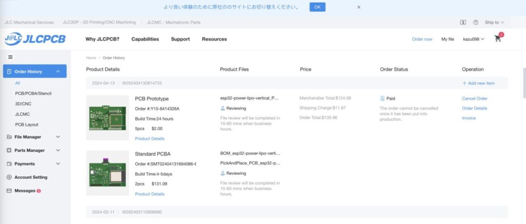
The order was successfully placed.
The contents of the order can be viewed at a glance in the “Order History” tab. In the “Order Status” section, you will see a link “Shipment status”, which you can click to view the shipment tracking.
It usually takes about one week to 10 days from the time the order is placed to the time it arrives.


コメント